Analog Signal Conditioning for a Microcontroller

Table of Contents
A PCB designed to enable a microcontroller to sample up to 3 ± 10V signals, commonly found on industrial sensors. Each channel has an adjustable gain, adjustable offset and an active clipper to protect the ADC on the microcontroller. The board also contains an analog output calibration stage for a DAC, again with adjustable gain and offset.
Analog Input #
A single channel for the analog input looks like the following:

The input is connected to the board via a terminal block. The first stage is a voltage follower / buffer amplifier (U1A) that provides a unity gain high impedance input for the signal.
To scale the signal, which requires a gain less than 1, an inverting amplifier is used (U1B). The configuration with a 10k resistor in the forward path and a 1k and 10k trim pot in the feedback path gives an adjustable gain between -0.1 and -1.1.
Next is another inverting amplifier (U1C) used to sum the previous signal with an adjustable offset. The offset can be varied between -7.5 and 0V by another trim pot (negative since the previous signal has been negated). The offset voltage is sourced from a buffer amplifier (U1D) so no extra current is drawn from the trim pot, which would effect the set voltage.
Signal Clipping #
The output voltage from the previous stage could potentially be outside the operating region of the microcontroller, typically 0-3.3V or 0-5V. If a trim pot was set incorrectly or the original signal went out of the expected range, the ADC on the microcontroller could be damaged. To prevent this, an active clipper circuit is used, formed by U7C and U7D in the schematic.
Firstly, a 1K resistor is used on the input to limit the current and enable a voltage drop from the previous section if required. For the low voltage limit, the non-inverting input of U7C is tied to ground and the inverting input connected to the input signal, with a diode in the feedback path. Whilst the input voltage is above 0V, the amplifier has no affect on the signal as the diode is reverse biased. When it drops below 0V, the diode conducts and the amplifier sources current across the input 1k resistor to increase the voltage to 0V.
A similar process occurs for the high voltage limit with U7D, except if the input signal is greater than the voltage on the non-inverting input, the op-amp will sink current to bring the voltage down.
Finally a buffer amplifier is used to reduce the output impedance of the circuit for better performance with an ADC.
Analog Output #
For this project it was also required to scale and offset a voltage signal from a microcontroller DAC. A similar dual inverting op-amp configuration was used with trim pots to change the offset between +-5V, followed by a gain of 0.5 to 1.5. The aim was to convert a 0 - 3.3V signal to 1 - 5V in order to drive a mosfet in its ohmic region, to control power dissipation.

PCB #
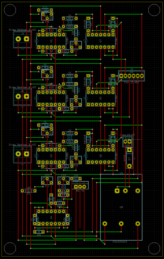
Since this was a one-off part with simple through-hole components, a stripboard was more than adequate to implement the design (after testing on a breadboard to confirm it works). As a bit of a KiCad practice and to limit the mistakes when soldering, I designed the layout first.

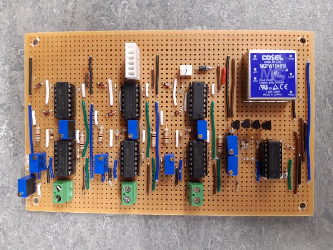
It fit just perfectly on the piece of stripboard I had. The red layer of the board is used to represent the traces (strips) already on the board, and the green layer are the wire jumps to be made. Although it was not followed exactly when the board was soldered, it was very useful to make sure I was doing it correctly.
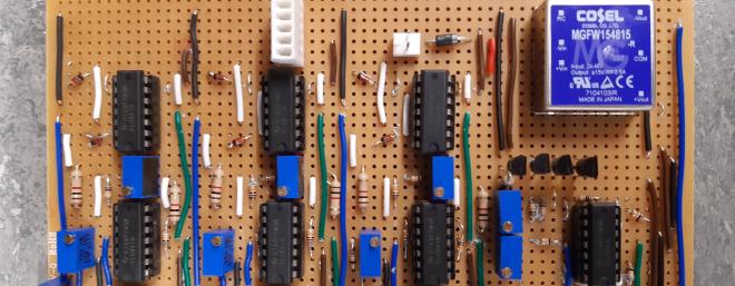
The final board has a +-15V supply module to power the op amps from a 24V supply, and the microcontroller can be connected via a 6-pin molex header.
